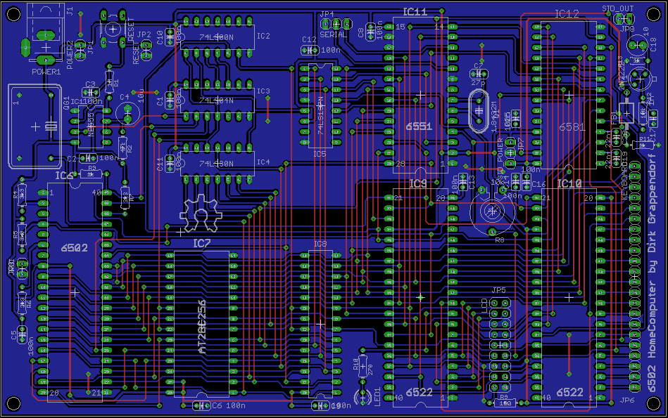
Printed Circuit Board
This is the final design that I used to create the actual PCB:
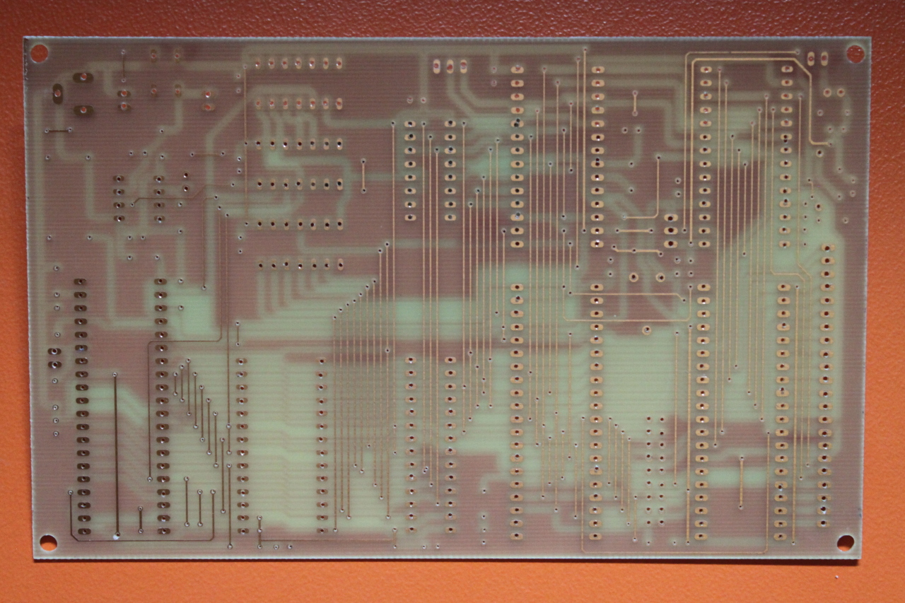
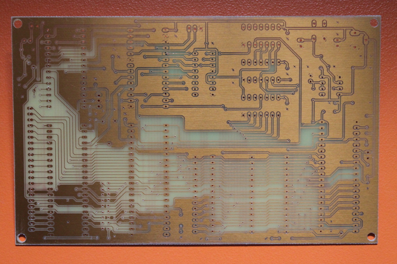
In my PCB production process i use transparent films and print the layout with an inkjet printer. In the following images you see the finished etched and drilled PCB:
Now soldering ~200 vias by hand. Sounds like a lot of fun!
After hours of soldering, here is the final result:
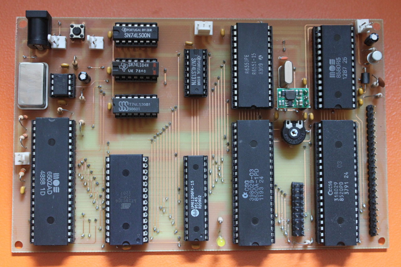
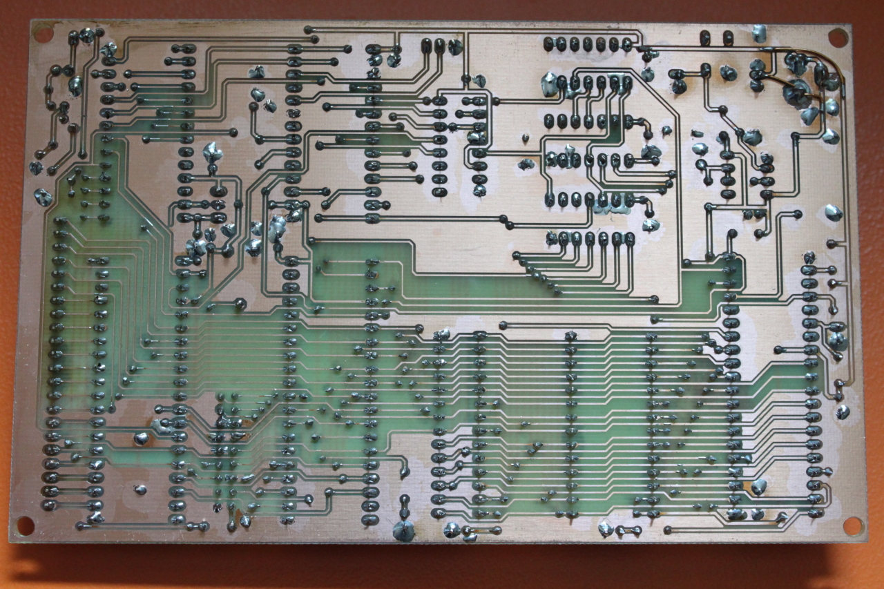
And as you can see in the upper right corner of the right picture, there is always at most one component that one has done wrong. In my case i selected the wrong part for the power socket which has the polarity interchanged. The inner pin needs to be connected to +5V. This is corrected in the final PCB layout file.
Between the ACIA and the SID above the LCD trimpot you can see the small board that contains the 5V to 9V boost converter .
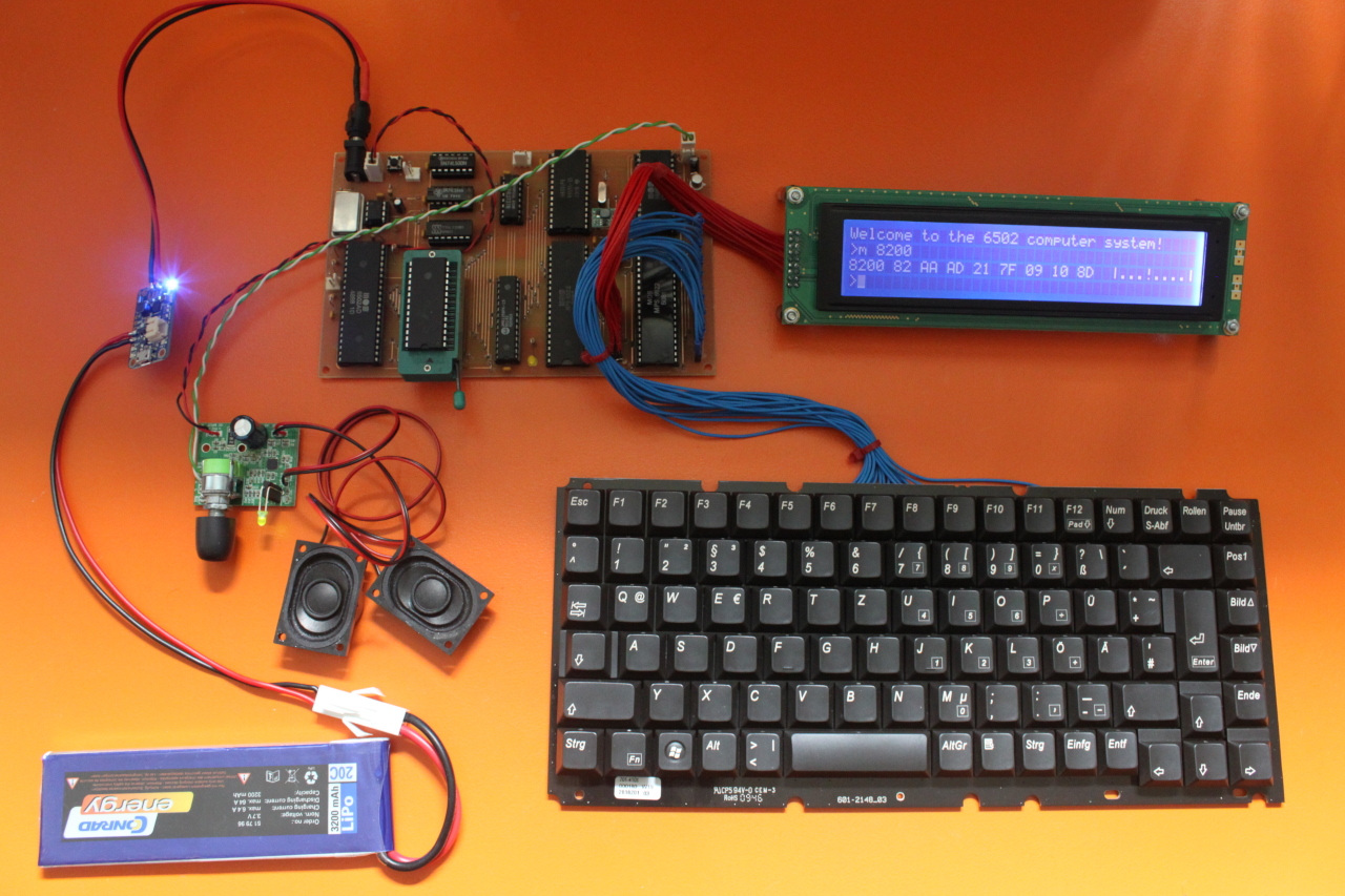
Here once again is the complete 6502 computer system. I extracted the electronics from the active speakers and replaced the big, clunky speakers with two smaller ones. I also added a LiPo-charger-to-5v-boost-converter from Adafruit and a single cell LiPo battery.