RAM
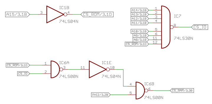
With only three 8-bit registers (A, X and Y) it would be quite difficult, if possible at all to write interesting programs. Therefore we need RAM! And to differentiate between the RAM and the IO devices, we need more address decoding logic. I'll use a 32k static RAM which will be visible in the lower half of the address space. But in the highest 256 bytes we will not select RAM but the IO devices instead. So our IO device registers will be accessible at the addresses $7F00 to $7FFF. Here are the equations for the three main chip select signals (A ! before a signal name denotes a low-active signal, ¬ is the negation):
!CS_ROM = ¬ A15
!CS_IO = ¬ (!CS_ROM ∧ A14 ∧ A13 ∧ A12 ∧ A11 ∧ A10 ∧ A9 ∧ A8)
!CS_RAM = ¬ (!CS_7F00 ∧ !CS_ROM ∧ ϕ2)
And the memory map looks like this:
| Addresses | Type |
| $0000 - $00FF | RAM - Zero page |
| $0100 - $01FF | RAM - Stack |
| $0200 - $7EFF | RAM |
| $7F00 - $7FFF | IO |
| $8000 - $FFFF | ROM |
The !CS_IO signal can be generated with an 8-input NAND gate 74LS30 .
I first built this modified circuit, changed the ACIA register definitions accordingly and verified that my hello world program still works.
Then i built the !CS_RAM circuit using a 74LS00 NAND and one 74LS04 inverter and connected a 61256 32k x 8 SRAM to the address and data buses. !CE and !OE are connected to !CS_RAM and !WE to R/!W.
Schematic
Breadboard construction
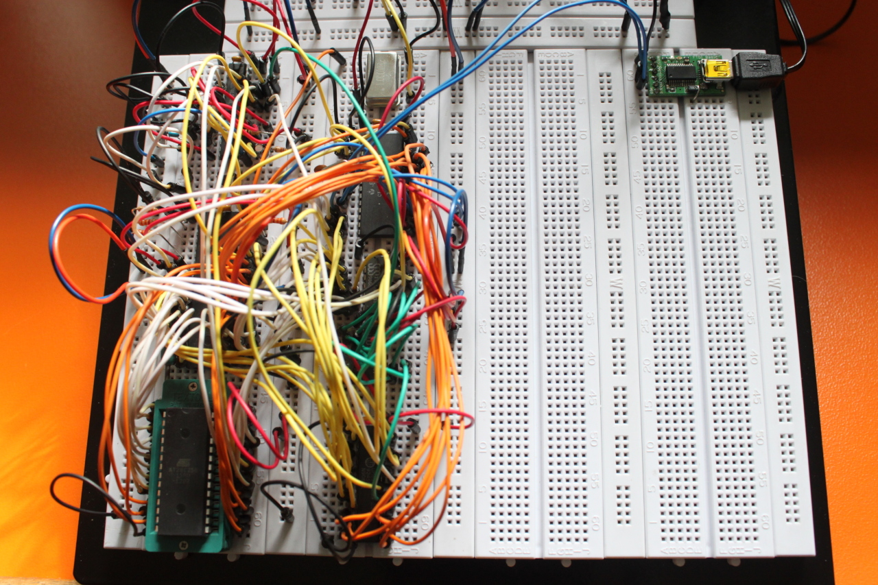
It's getting a little bit messy. Cables everywhere. Below the ACIA you can just barely see the two 74 logic ICs for the address decoder. At the bottom next to the EEPROM is the 32kB SRAM.
Simple test program
This is just a small extension of the program of the previous ACIA part. Instead of directly sending the "Hello World!" string to the serial port, i first copy this string to RAM (string_data). When sending the string, the characters are now fetched from the RAM locations. If this works, it is a first simple confirmation that our RAM and address decoding logic works.
                  .setcpu "6502"
                  ACIA_DATA = $7f00
                  ACIA_STATUS = $7f01
                  ACIA_COMMAND = $7f02
                  ACIA_CONTROL = $7f03

                  .segment "VECTORS"

                  .word   nmi
                  .word   reset
                  .word   irq

                  .data

string_data:
                  .code

reset:            jmp main

nmi:              rti

irq:              rti

main:
init_acia:        lda #%00001011        ;No parity, no echo, no interrupt
                  sta ACIA_COMMAND
                  lda #%00011111        ;1 stop bit, 8 data bits, 19200 baud
                  sta ACIA_CONTROL

                  ldx #$ff
copy_string:      inx
                  lda text,x
                  sta string_data,x
                  bne copy_string

write:            ldx #0
next_char:
wait_txd_empty:   lda ACIA_STATUS
                  and #$10
                  beq wait_txd_empty
                  lda string_data,x
                  beq read
                  sta ACIA_DATA
                  inx
                  jmp next_char

read:
wait_rxd_full:    lda ACIA_STATUS
                  and #$08
                  beq wait_rxd_full
                  lda ACIA_DATA
                  jmp write

text:             .byte "Hello World!", $0d, $0a, $00
We also need to extend our memory layout configuration. The following file defines the RAM area as the DATA section and the first 256 RAM bytes as the ZEROPAGE section.
MEMORY
{
        ZP: start=$0, size=$100, type=rw, define=yes;
        RAM: start=$0200, size=$8000, type=rw, define=yes;
        ROM: start=$8000, size=$8000, type=ro, define=yes, fill=yes, file=%O;
}

SEGMENTS
{
        ZEROPAGE: load=ZP, type=zp, define=yes;
        DATA: load=RAM, type=rw, define=yes;
        CODE: load=ROM, type=ro;
        VECTORS: load=ROM, type=ro, offset=$7ffa;
}
PCB
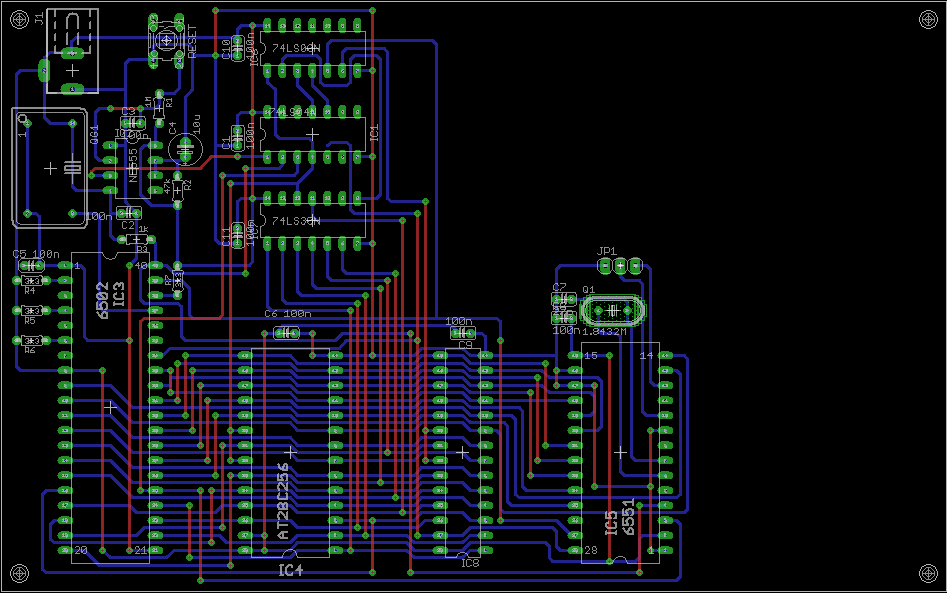
Forget all about what I've said about starting to lay out your board as early as you can. ...No, just kidding... Only if you don't know what you want to build from the beginning, chances are high that you might need to completely redesign your PCB. As you can see in the above picture, the only chance to layout even such a simple circuit as the one described here, is to use a two layer board with lots of vias. This is a classic layout scheme: (mostly) horizontal traces on the bottom and (mostly) vertical traces on the top (or vice versa).