The Microprocessor
We have a clock and a reset signal and now we can add the 6502 CPU . But wait. We have no ROM, no RAM and no IO devices. How on earth can the CPU do anything useful that we can test and measure? Well, the answer is by doing nothing!
When the processor is powered up, it reads the contents at the addresses $FFFC and $FFFD, the reset vector. Then it starts program execution at the address denoted by this vector. It reads an opcode from this location and decodes and executes this operation. And there is a special operation that does exactly nothing: NOP or $EA.
So if we wire the data bus to always read $EA, this is what happens: For the 6502 there seems to exist a single huge ROM containing nothing more than $EA. It reads $EAEA from the location $FFFC/$FFFD and starts program execution here. It reads $EA from $EAEA and executes the NOP operation. Then the program counter is incremented to $EAEB and another NOP is read and executed again. And this is repeated until the the cows come home. Since the program counter is incremented by one after each NOP execution, we should be able to measure square wave signals with continuously halved frequency on the address lines A15 to A0.
Here is the MOS 6502 wikipedia page .
And here is a MOS 6500 family data sheet .
Schematic
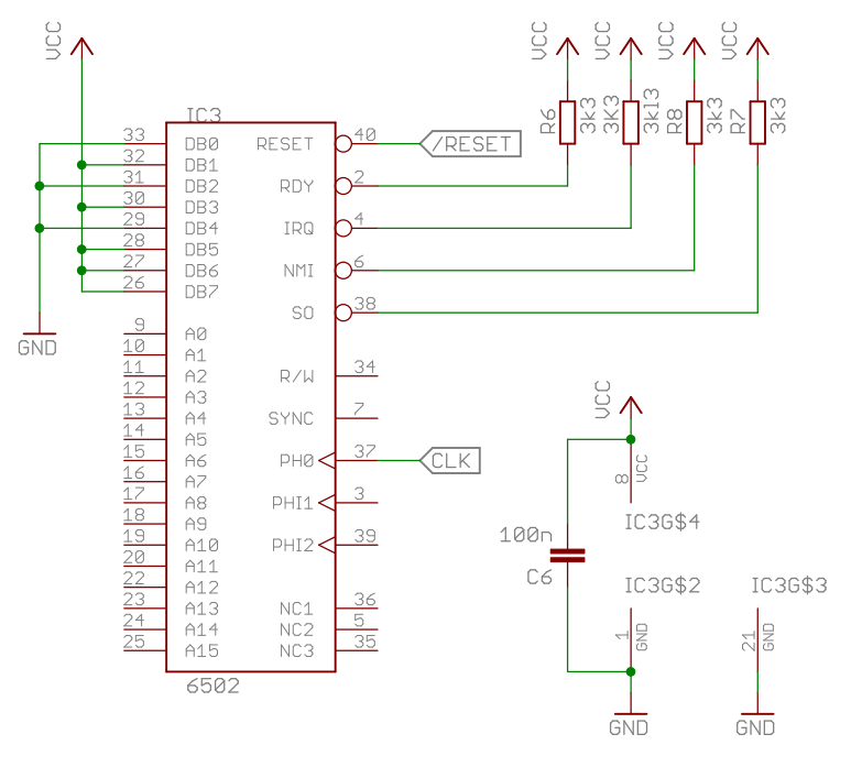
As you can see, the data bus lines are either connected to VCC or to GND. This works, because we ensure that the processor only reads from the data bus (you could make this more secure by inserting resistors into these connections).
Breadboard construction
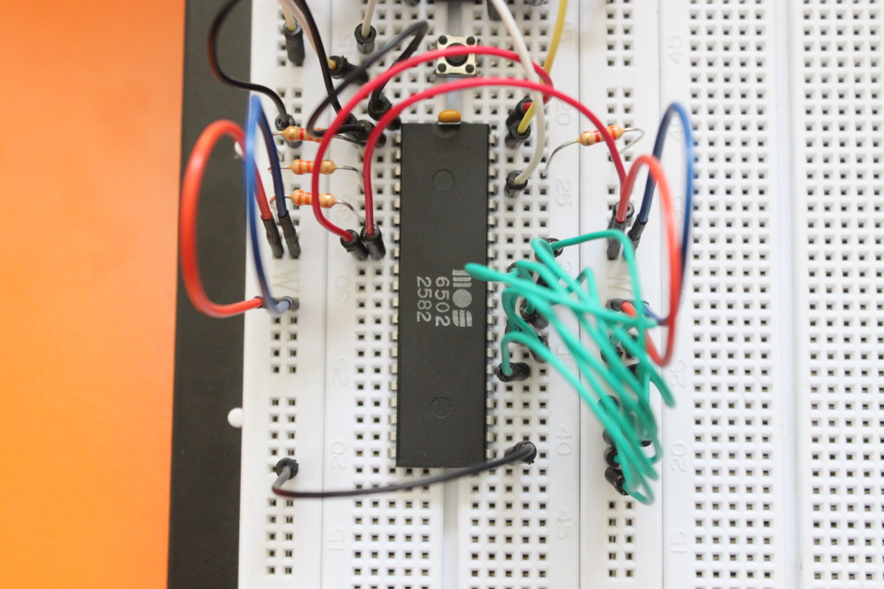
The 6502 is connected to the power supply, the reset signal and the clock signal. The data bus lines are connected to GND and +5V in a way, so that the CPU always reads the byte $EA.
Measurements
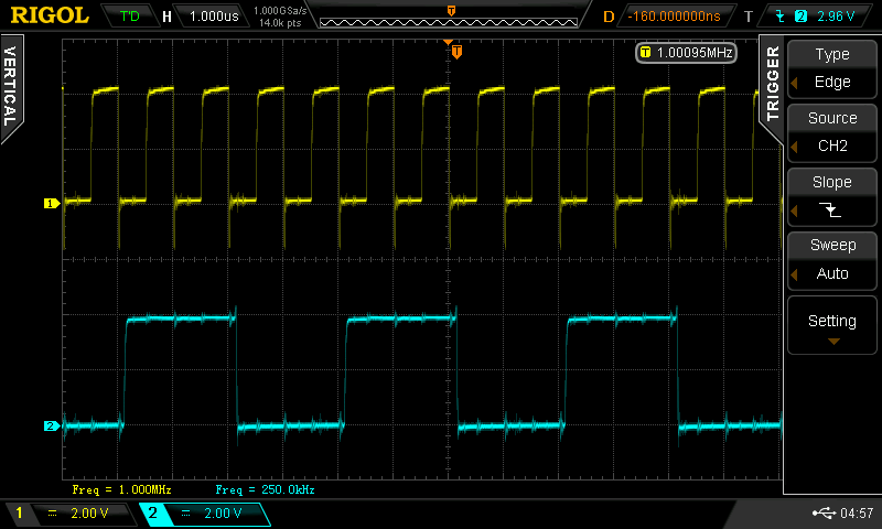
Channel 1 shows the 1 MHz system clock, Channel 2 is connected to A0. A NOP operation needs two clock cycles. In the first cycle the instruction is fetched from memory and in the second cycle it is decoded and executed. Therefore A0 changes every 2 microseconds and the frequency of the A0 signal is 250 kHz.
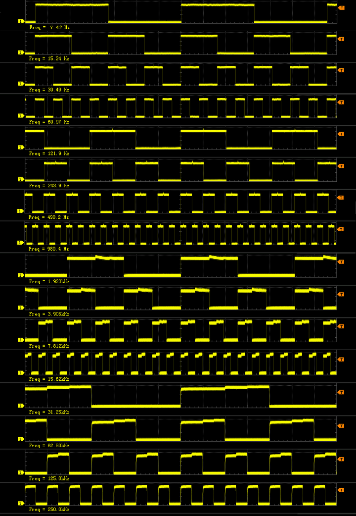
Here's the measurement of all address lines, A15 at the top, A0 at the bottom. I've changed the time base for every four address lines, to get somewhat accurate frequency measurements. As you can see, every address line divides the frequency by 2 because the program counter is incremented by 1 after each NOP operation.
PCB
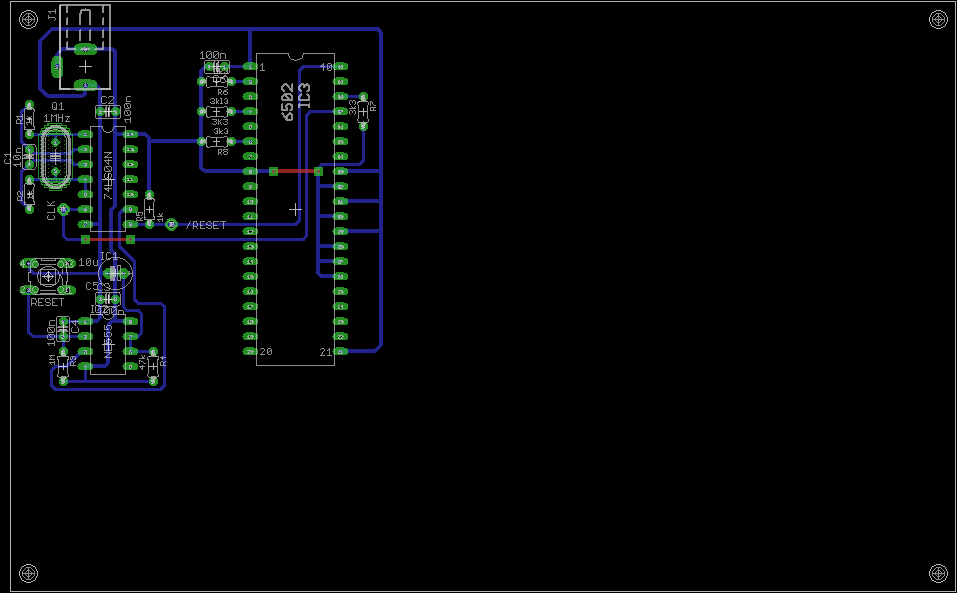
On the PCB the 6502 CPU is placed next to the clock and reset circuitry.