VIA (Ports and Timers): Blinking LED
Contents | Back: Monitor program | Next: LCD Display
In this part we will add a 6522 VIA to our computer system to implement the real "Hello World!" program of microcontroller electronics: a blinking LED!
Currently the ACIA's !CE is connected directly to !CS_IO, so that it is mirrored 64 times into the 256 bytes of the $7F00 to $7FFF IO space. If we want to connect multiple IO devices, we need to divide the IO address range into different parts, where each on has its own chip select signal. I have a 74LS137 3-line to 8-line decoder laying around, which lets us connect 8 IO devices to our system. The circuit is quite simple:
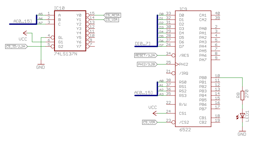
The decoder is only enabled if !CS_IO is low. Then A7, A6 and A5 are used to select one 32 byte block out of the 256 IO bytes. So we can connect 8 IO devices and each one could hold up to 32 registers (The ACIA only has four, the VIA has 16, but a SID has 29 registers). The signal Y0 ($7F00- $7F1f) goes to !CS_ACIA and the signal Y1($7F20-$7F3F) goes to !CS_VIA.
The VIA needs to be connected to the data bus, ϕ2, chip select and the four address lines A0 to A3.
The LED is connected to port pin PB0 and with a current limiting resistor to ground.
Breadboard construction
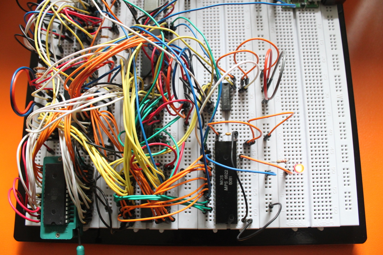
More cables, ICs and an LED. But apparently this extension is not that complicated.
Program
We set all lines of port B to output, set the pins low then wait some time, set the pins high, wait again and repeat indefinitely.
            .setcpu "6502"

            VIA_DDRB = $7f22
            VIA_ORB  = $7f20

            .segment "VECTORS"

            .word   nmi
            .word   reset
            .word   irq

            .code

reset:      jmp main

nmi:        rti

irq:        rti

main:       lda #$ff
            sta VIA_DDRB
loop:       lda #$00
            sta VIA_ORB
            jsr delay
            lda #$ff
            sta VIA_ORB
            jsr delay
            jmp loop

delay:      ldx #200
@delay2:    ldy #0
@delay1:    dey
            bne @delay1
            dex
            bne @delay2
            rts
PCB
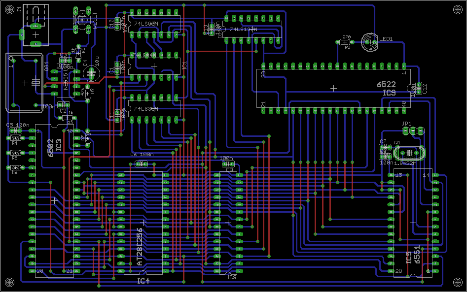
I needed to move the ACIA to the right to get all lines to the VIA. Obviously this layout needs some rework to make room for more components.